To complete this workshop, you will need:
- Fusion 360
- A Mouse connected to your computer
In this part of the workshop you will learn how to use Fusion 360 to create a simple circuit schematic. We will use a variation on the environment monitor from M,D,B Workshop 4 as our example circuit.
What You'll Learn
- Installation
- Creating a new project and schematic
- Adding libraries to Fusion 360/Eagle
- Creating a new project and schematic
- Adding parts to your schematic
- Zooming in and out
- Moving parts around the schematic
- Connecting parts
- Final Schematic
- Running an ERC Check
You should have already installed Fusion 360 during Sensor Data Visualisation module and you should already have an educational Autodesk account from when you installed Fusion 360, so use that account to sign in when you start Fusion 360. The PCB design component of Fusion 360 was previously distributed as a separate component known as Eagle CAD. However, Eagle CAD has now been fully integrated into Fusion 360 so no separate installation is required. However, for simplicity we continue to refer to the PCB design component of Fusion 360 as Eagle or Fusion 360/Eagle.
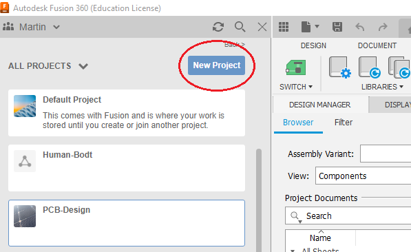
Create a new project called PCB-Design (see below).
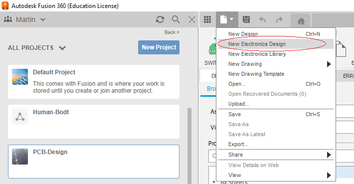
And then create a new file using the ‘New Electronics Design' option (see below)
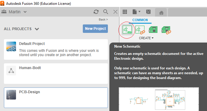
and add a new schematic to your new electronics design project (see below).
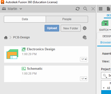
This will change the toolbar so that widgets appropriate for PCB design. Save the new file as ‘Schematic'. You should now see your Fusion 360 project populated with an Electronics Design project and within that a Schematic (see below).
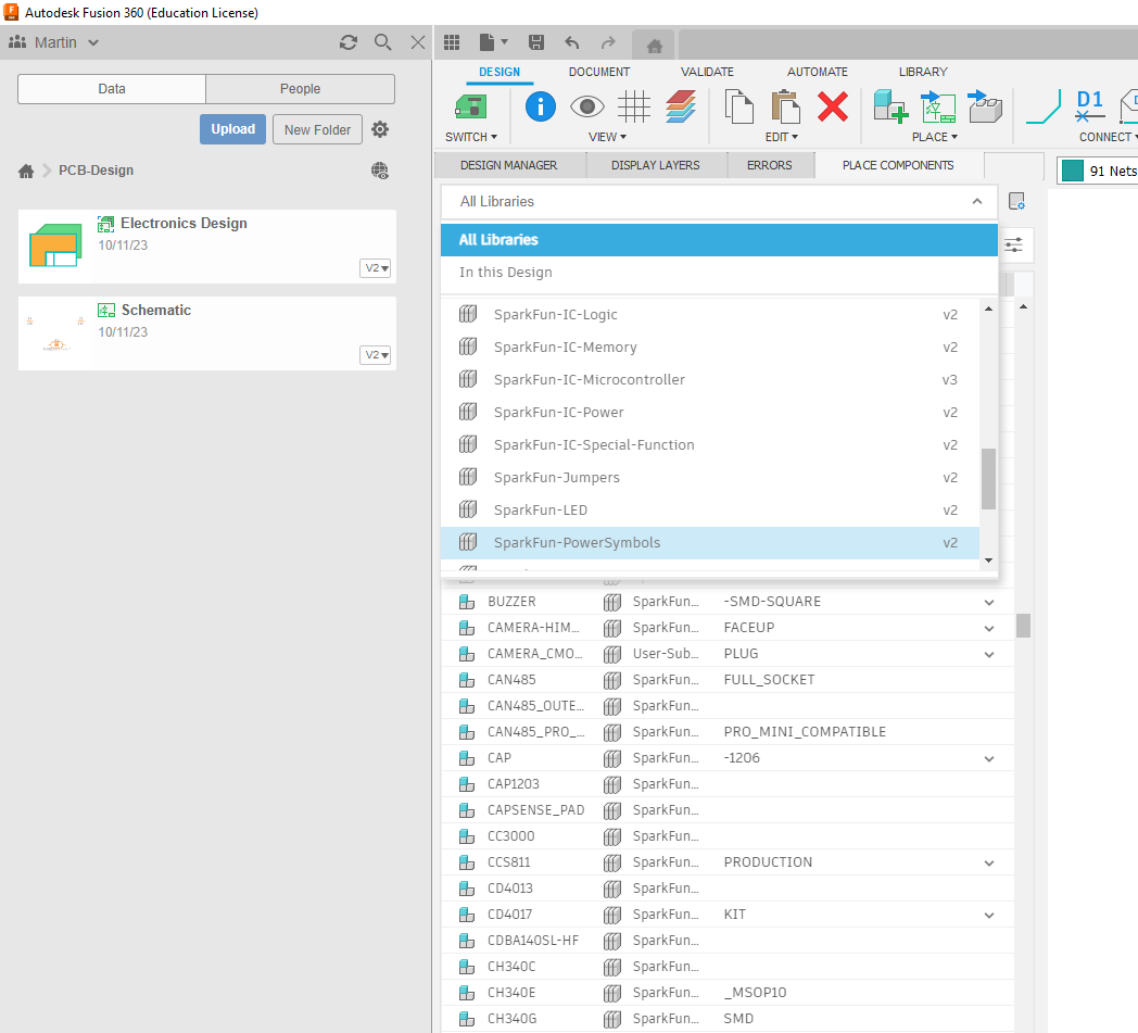
The Fusion 360/Eagle installation comes with a very comprehensive library of parts. In fact it is a bit too comprehensive and can be a bit overwhelming at first. So to simplify matters, for this project we will use the Spark Fun library only and hide the other libaries.
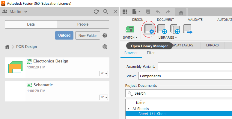
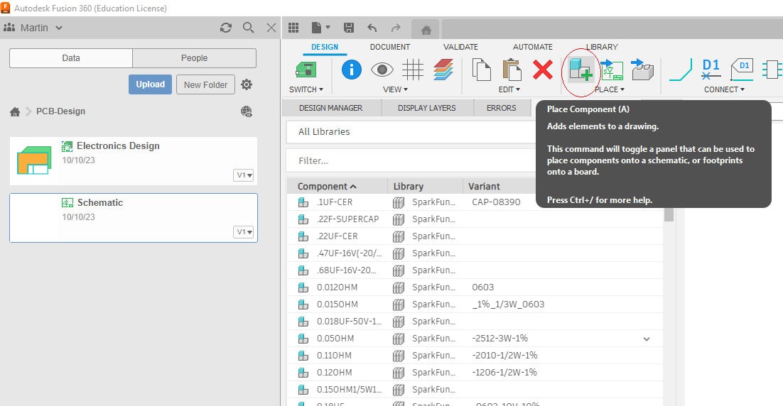
First, we will open the library manager. Select the library tab (see below)
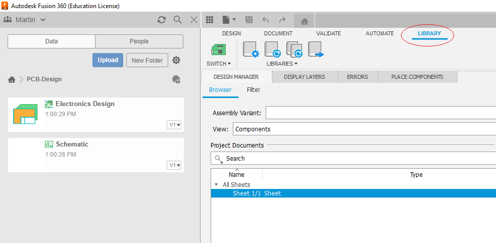
and open the Library Manager (see below)
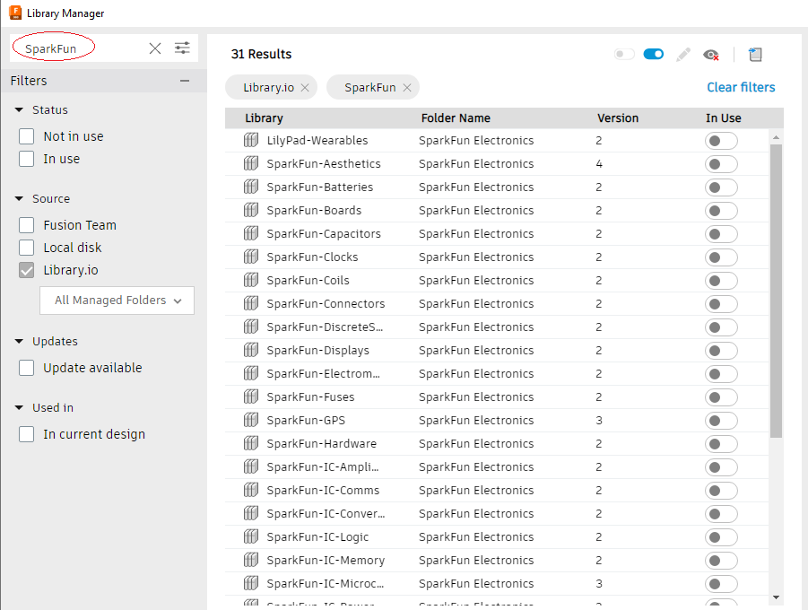
Make sure the Filters are set to Library.io which is the Autodesk library repository
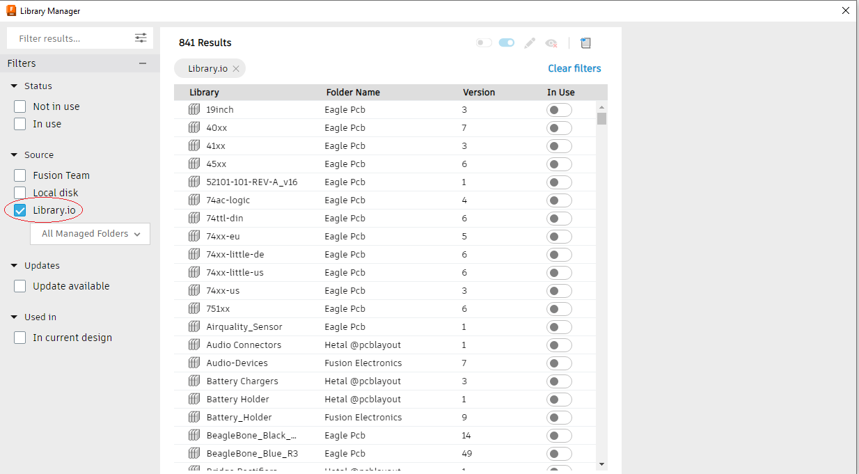
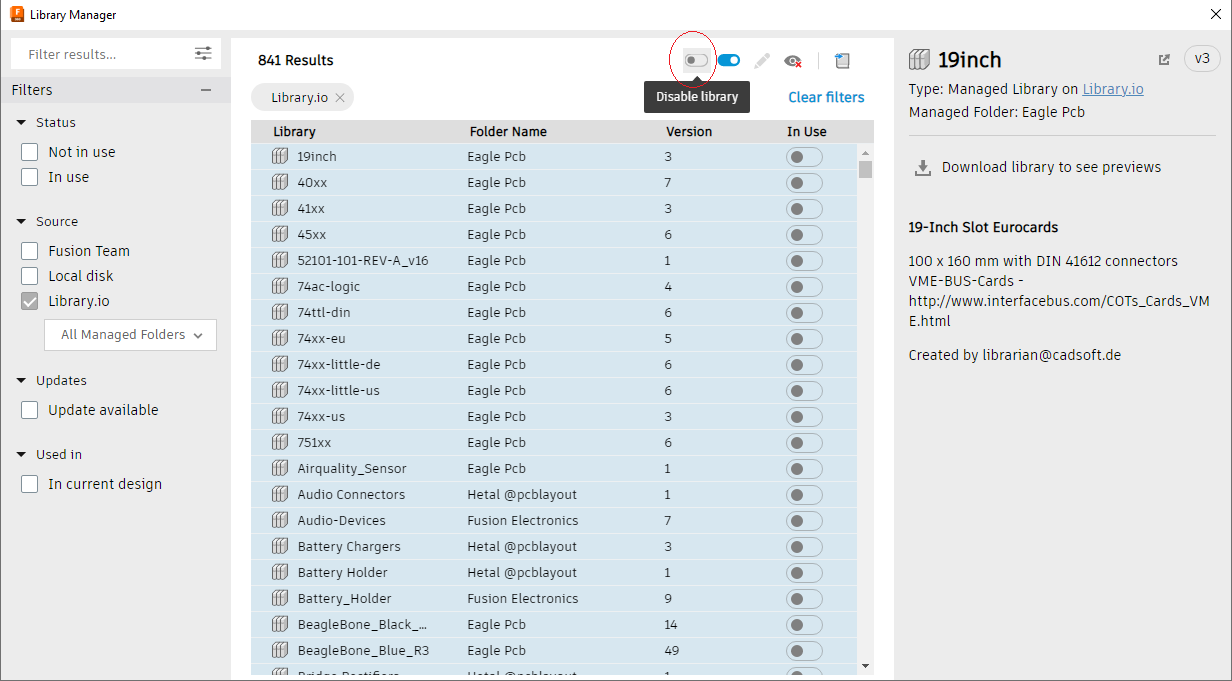
Next do a select all (Ctrl A) on the individual libraries and disable them (see below)
We are going to make use of a set of libraries from Spark Fun which should provide most of what we need. In the File Manager filter text box enter ‘SparkFun' (see below).
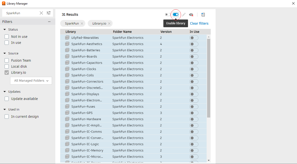
And then select all the filtered libraries (Ctrl-A) and enable them (see below)
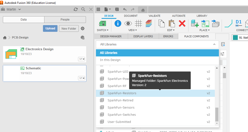
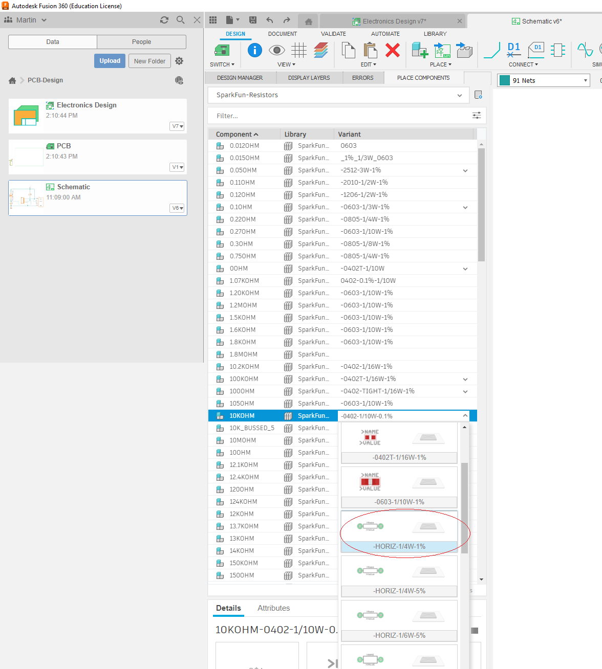
and change the library selection to just show resistors (see below)
then select a ‘Through the Hole' 10 KOHM resistor sub library
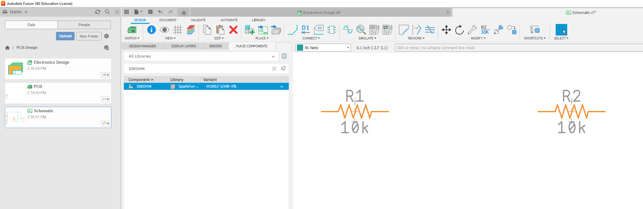
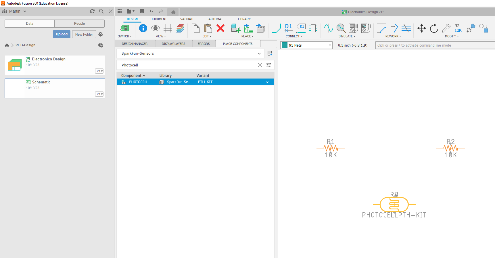
and drag it into the schematic, then left click your mouse to place it.
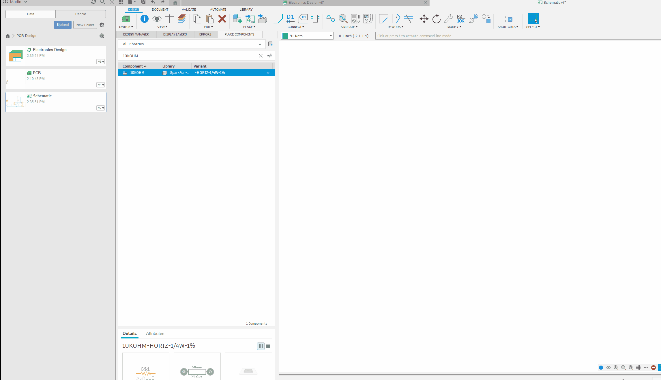
Move the mouse to a new location on the schematic and left click the mouse again to place a second 10KOHM resistor (see below). Then press Esc which will return you to a the parts library.
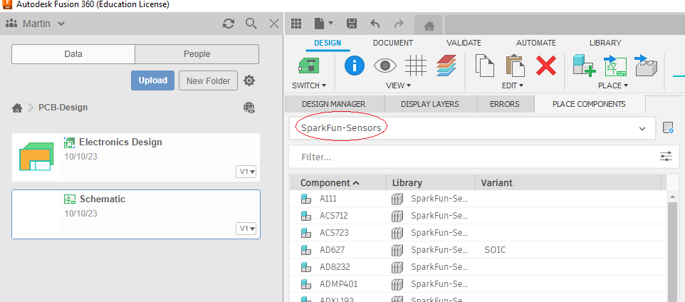
Now change the library selection to just show sensors (see below)
In the Filter text box type type Photocell (see below),
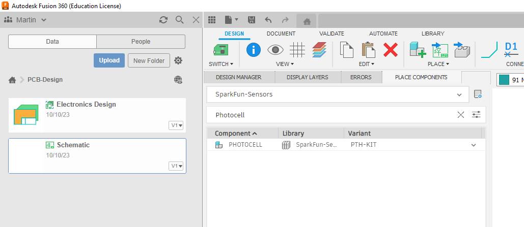
then select the photocell and drag it into the schematic, right click the mouse to place the photocell and use ‘Esc' to return to the parts library (see below).
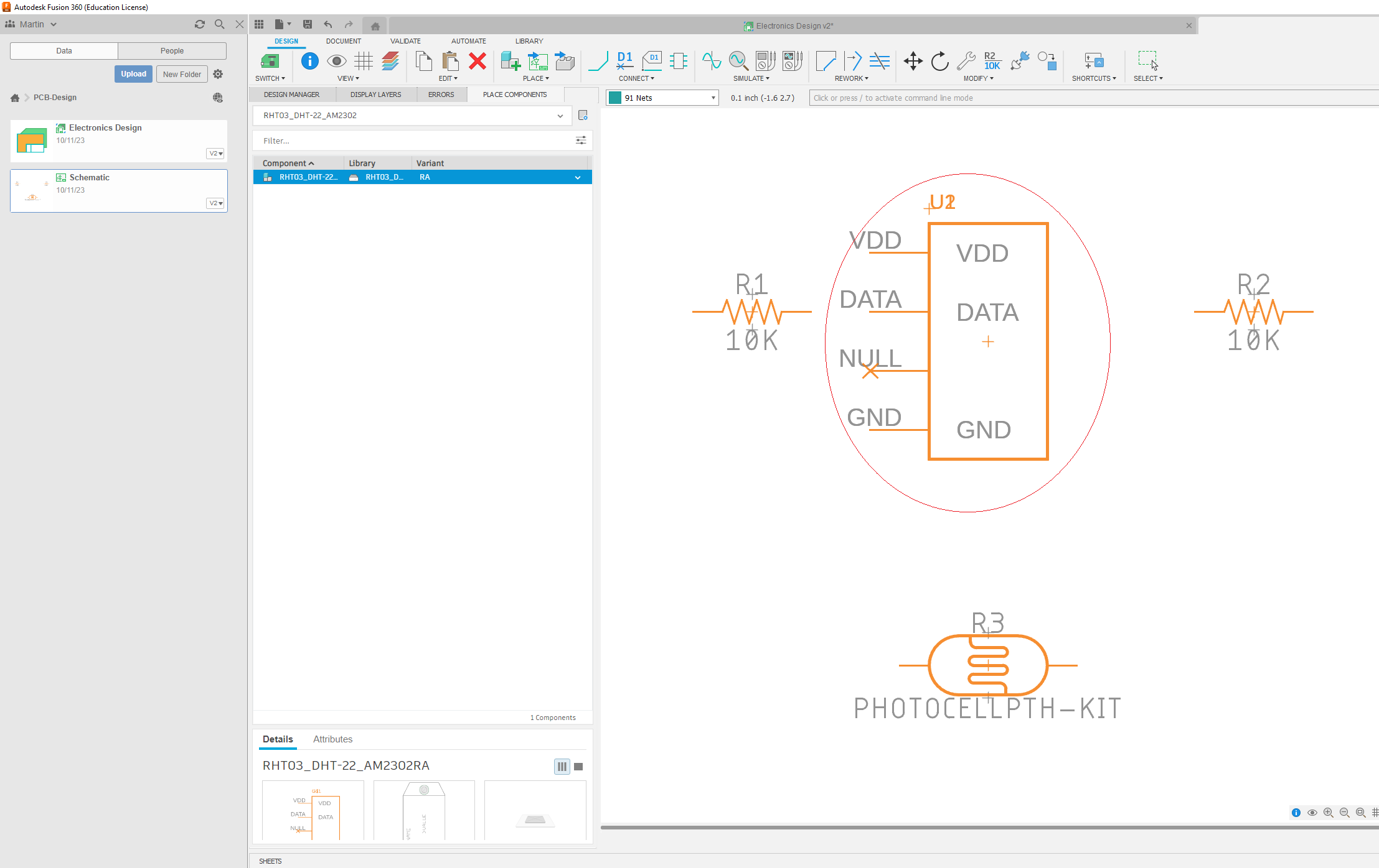
Now we want to add a DHT-22 part to the schematic. First we have to find an appropriate Eagle library containg the part, so we need to download another third-party library containing the DHT-22 part. Download and extract the zip file to a sensible location on your local file system.
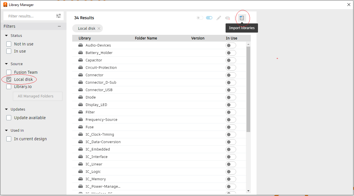
Open the Libray Manager, select ‘Local disk' in the left hand panel of Filters and click on the ‘Import libraries' button (see below)
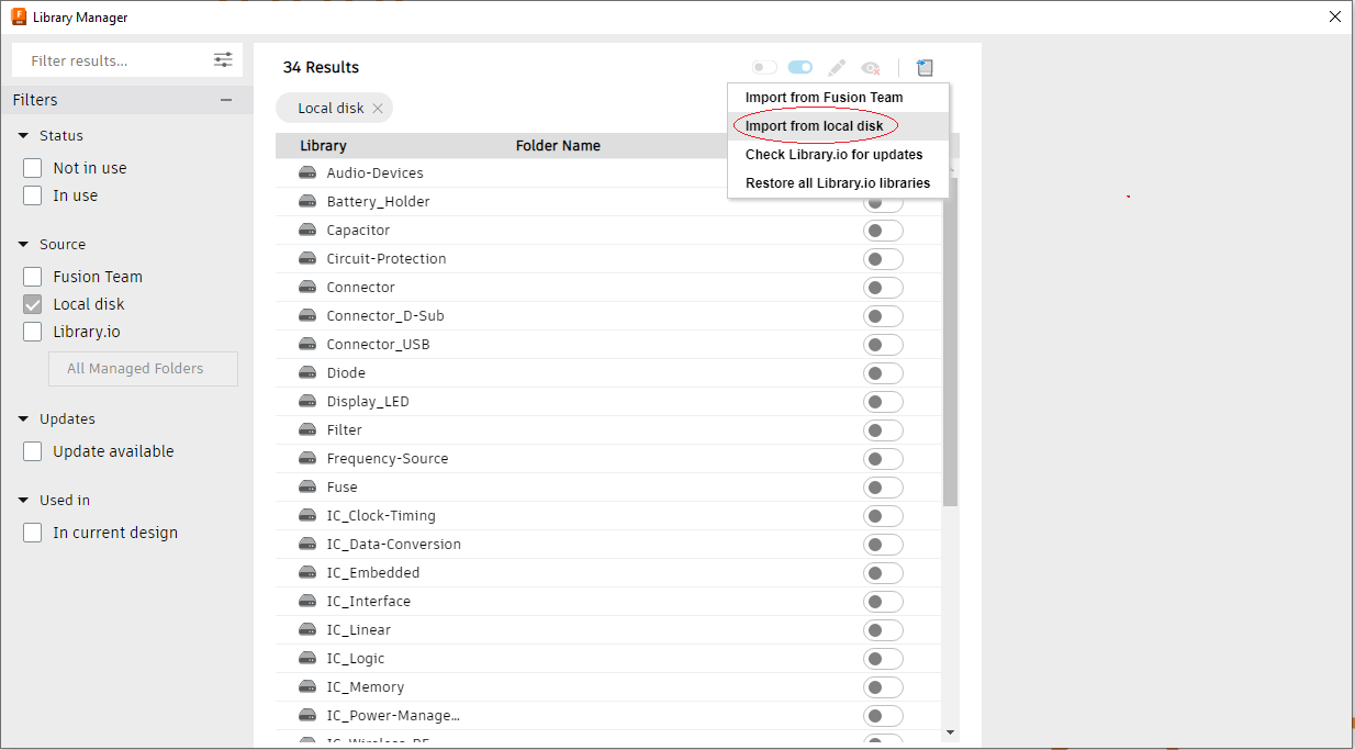
and select the ‘Import from local disk' option (see below)
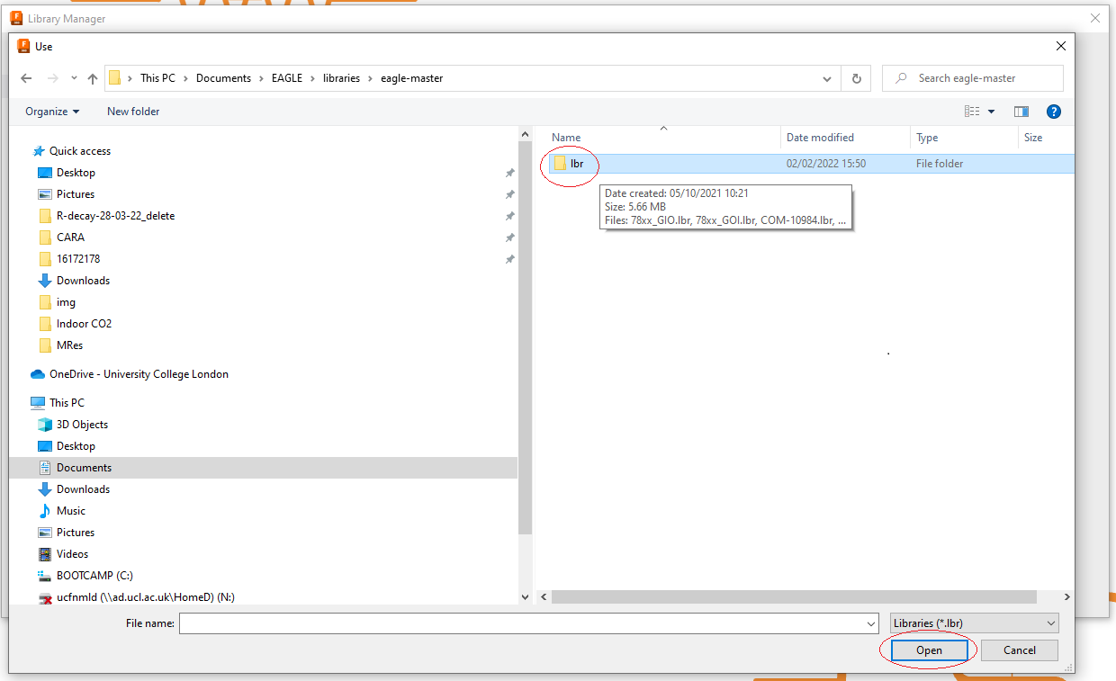
and navigate to the folder where you unzipped the third-party library, open that folder to locate the ‘lbr' folder and select ‘Open' (see below).
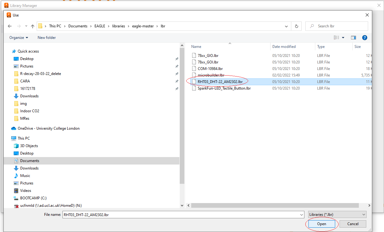
From the lbr folder select the library for the DHT-22 sensor (see below)
This will add the the DHT-22 to your parts library.
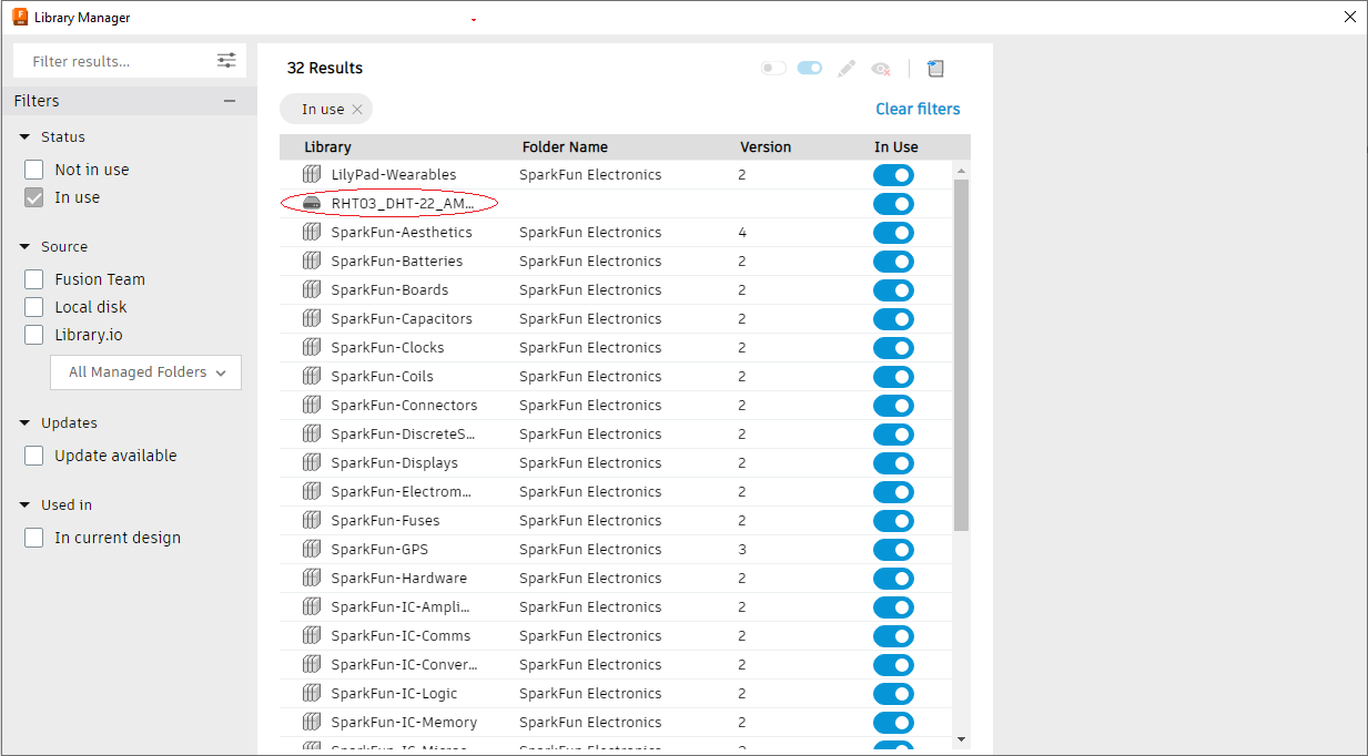
If you now select the ‘In use' Filter in the left-hand panel of the Library Manager, you should be able to see the DHT-22 part (see below).
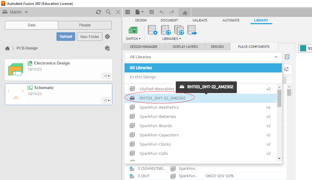
Now close the File Manager. From the Place Components tab select the DHT library (see below)
And drag the DHT-22 sensor into the schematic (see below)
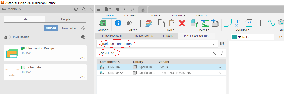
The final part to add is a set of header pins so we can connect our board to an Arduino. From the Place Components drop down list of in use libraries, select the SparkFun-Connector library and filter on CONN_04 (a sub-library of 4 pin connectors) (see below).
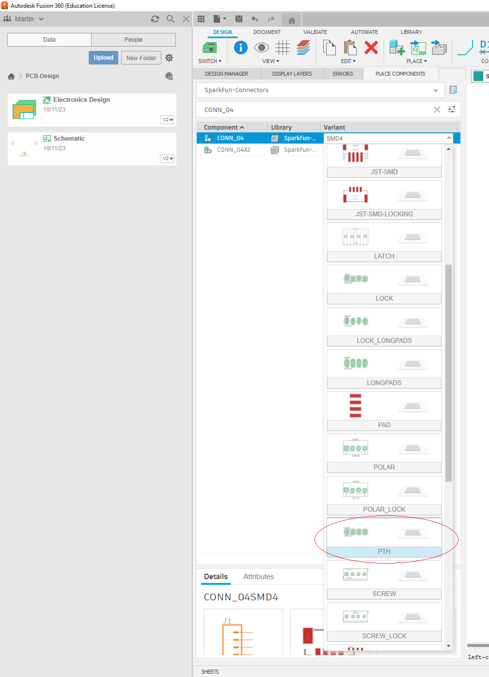
From the CONN_04 sub library look for the through the hole header pins (PTH) (see below).
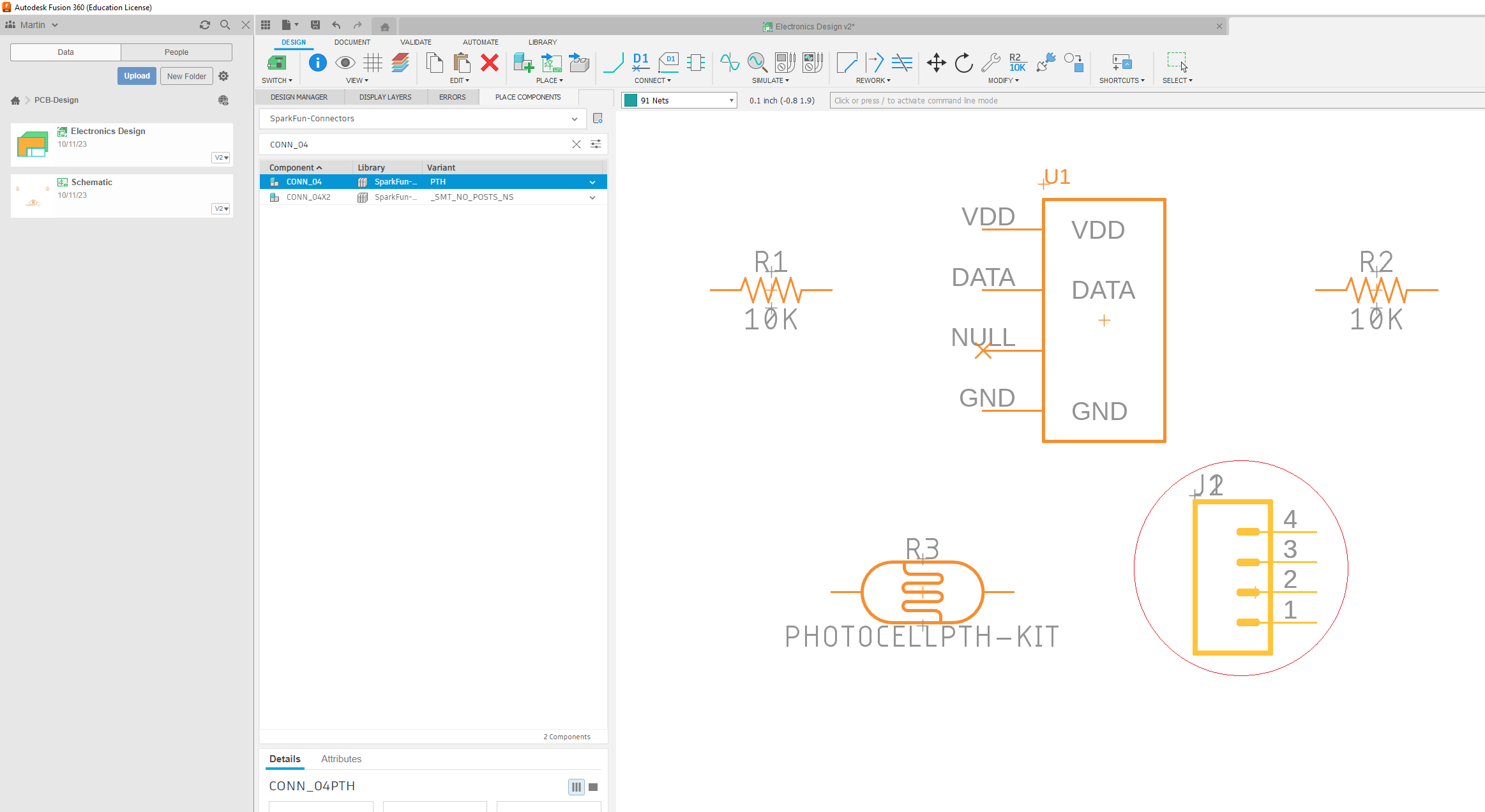
No drag the part into the schematic as before (see below)
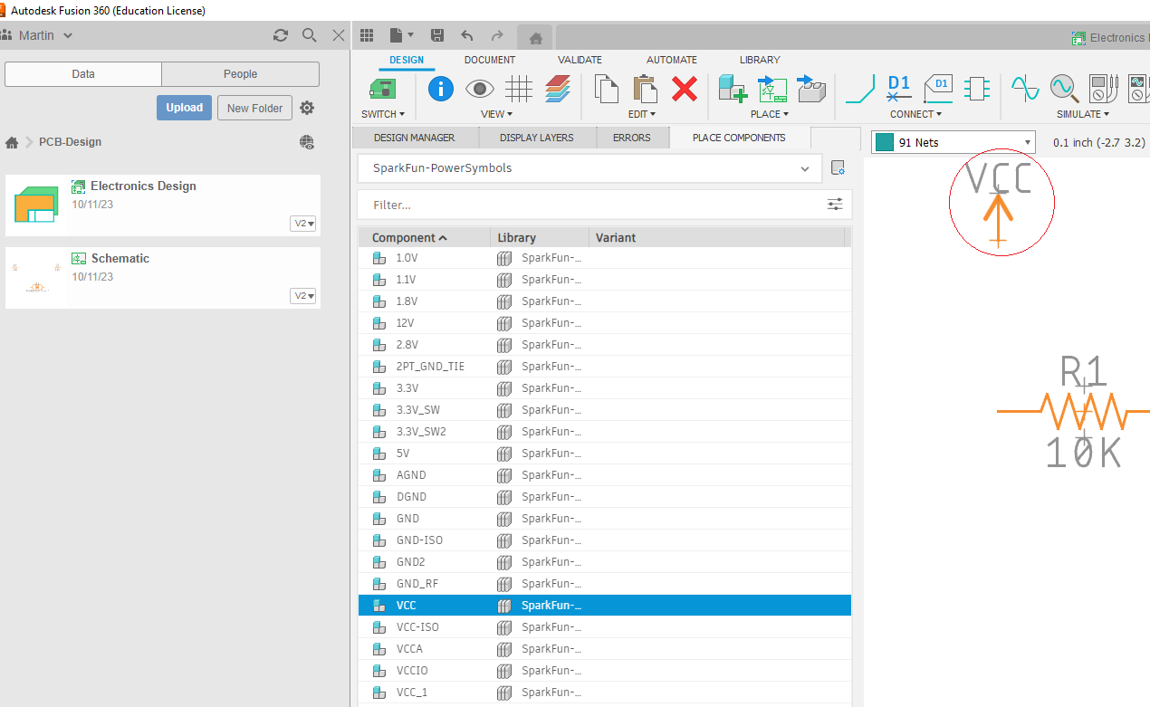
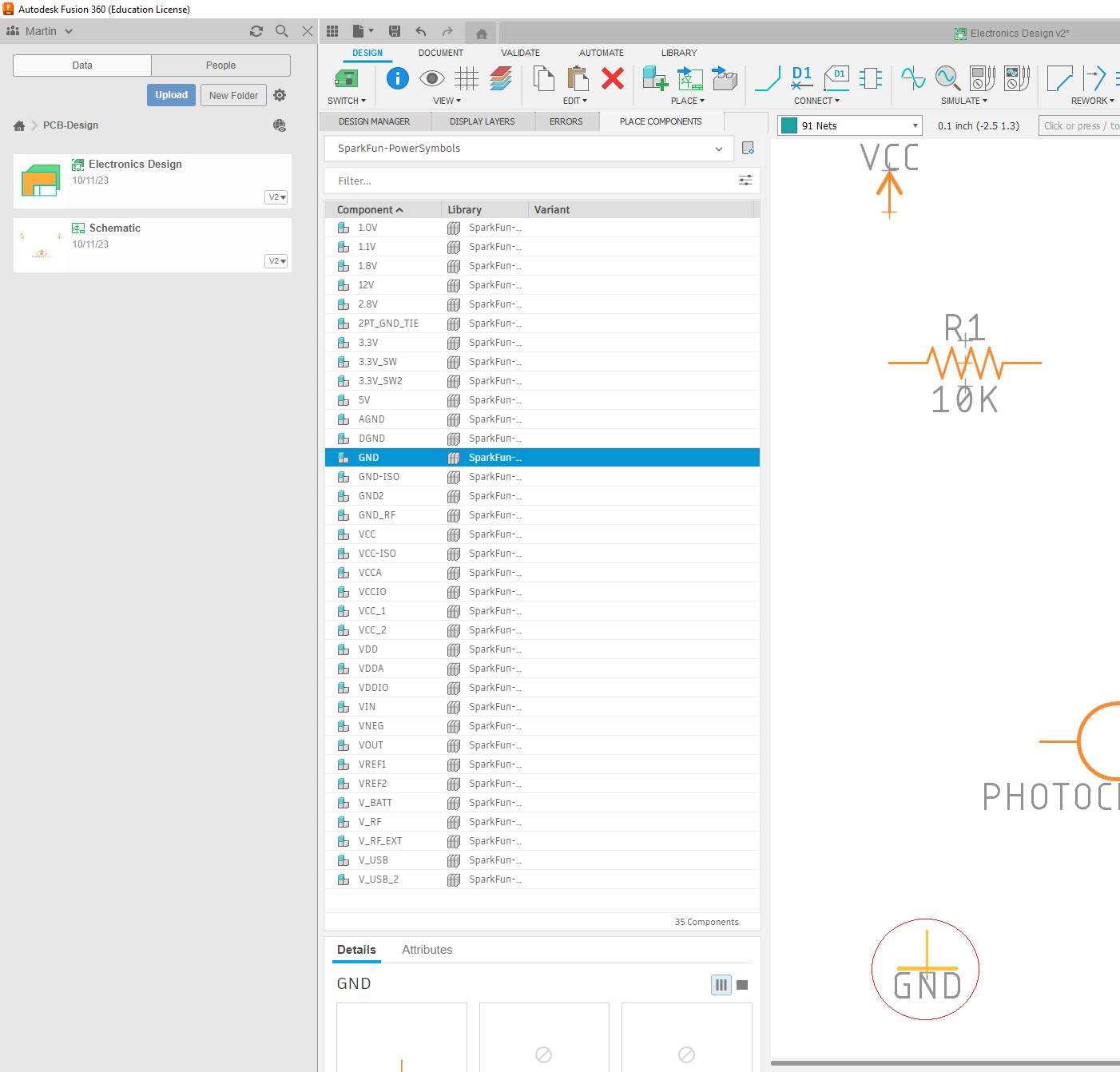
Although we have now added all the parts we need, it is useful to add symbols to represent the positive (Vcc) and negative (GND) power supplies. From the Place Components drop down list of in use libraries, select the SparkFun-PowerSymbols library (see below).
Add parts for Vcc
and GND to your schematic.
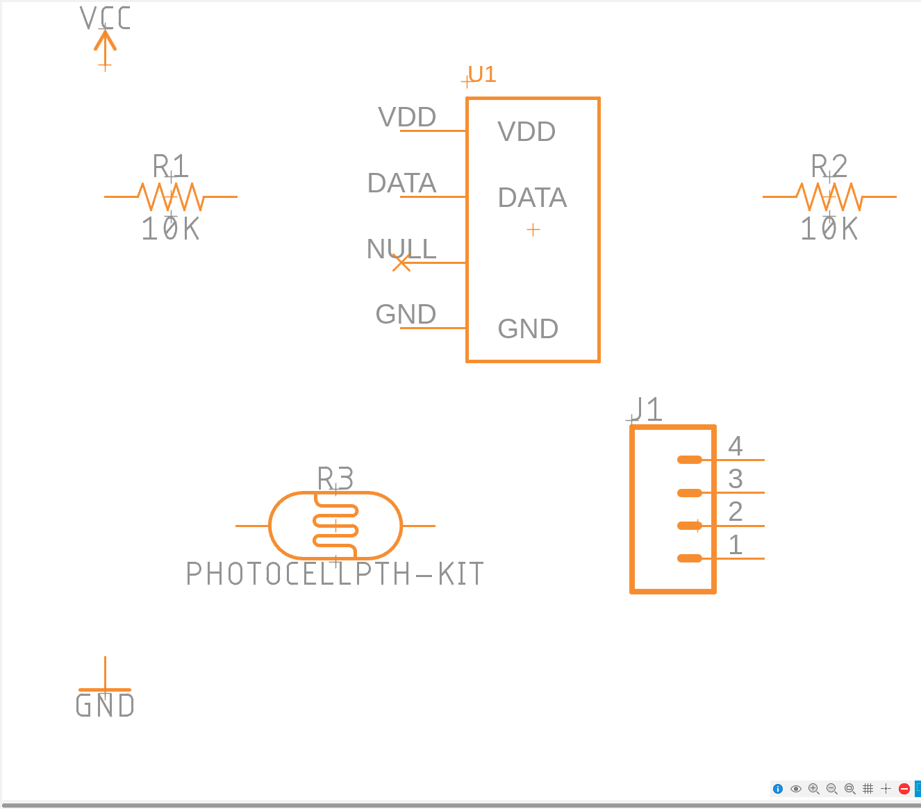
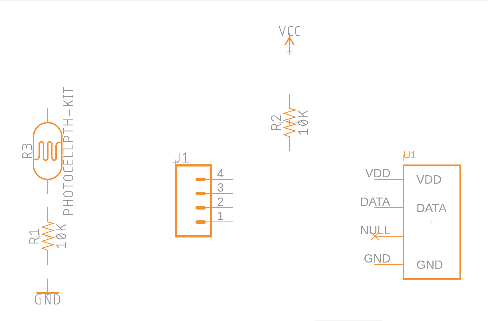
Your schematic should now look something like this
Save the schematic.
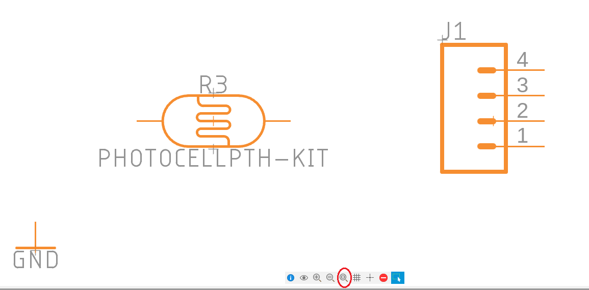
You may want to zoom in and out on your schematic. The image below highlights various zoom controls, perhaps the most useful being the Zoom to fit button (circled).
To move parts around the schematic, first click on the Move tool as shown below.
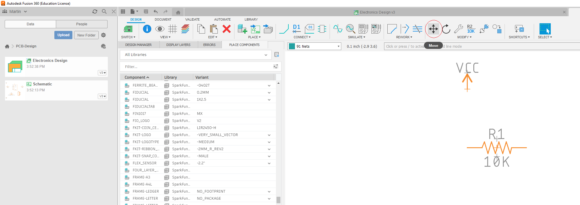
Then select the part you want to move by clicking on the cross hairs embedded in the part's symbol on the schematic and dragging it (see below).
To rotate a part, first click on the Rotate tool as shown below,
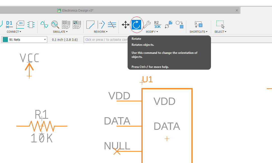
then click on the part you want to rotate on the schematic.
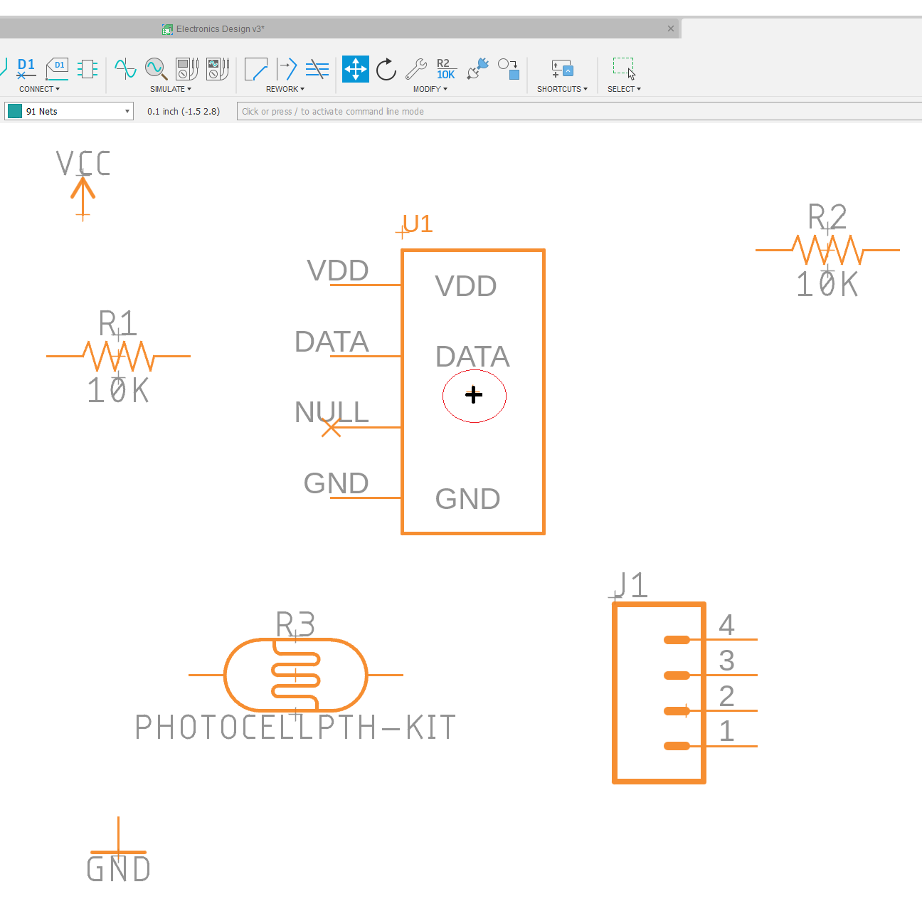
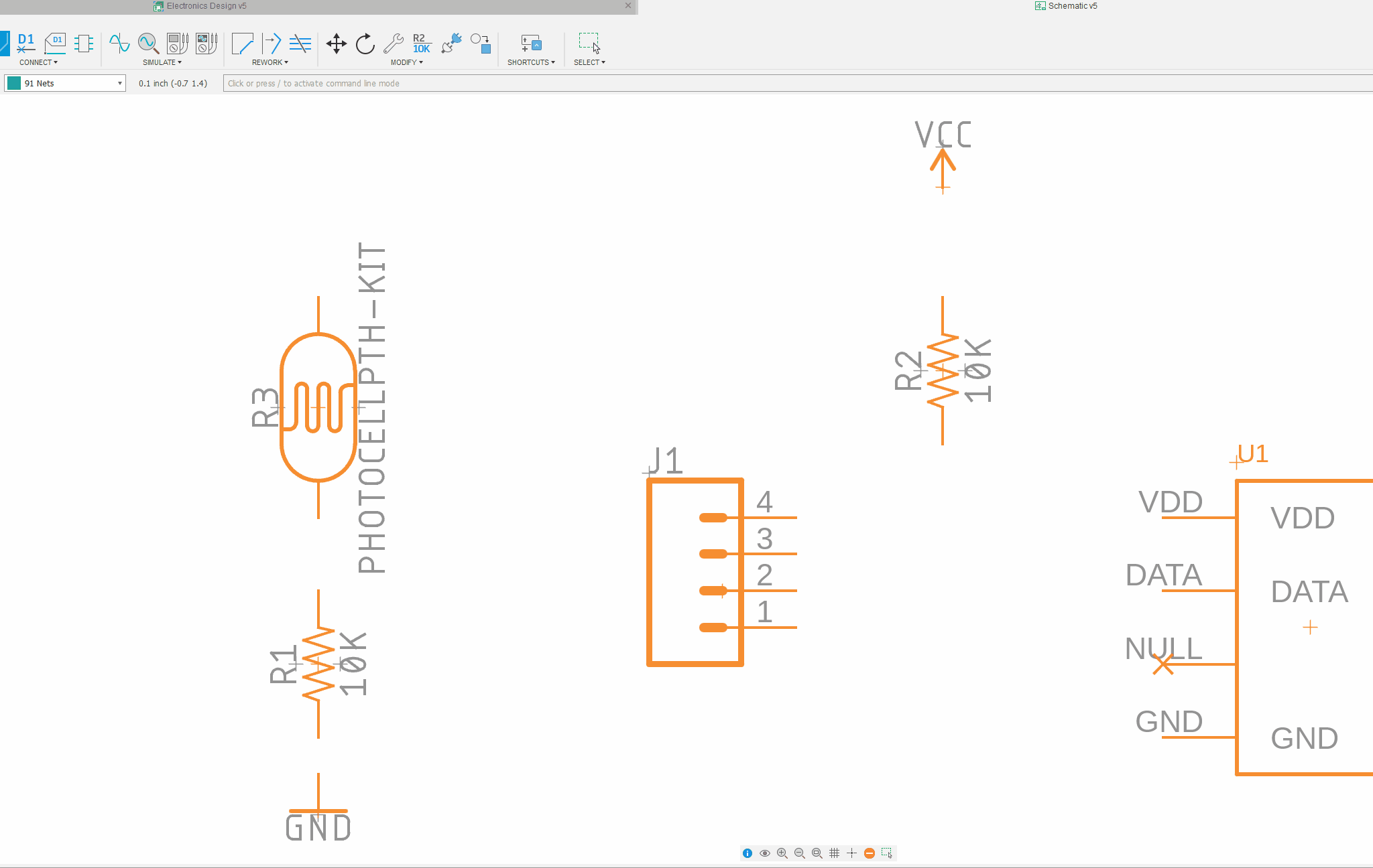
Using the Move and Rotate tools, one by one arrange the parts so your schematic looks something like this (see below).
Save the schematic.
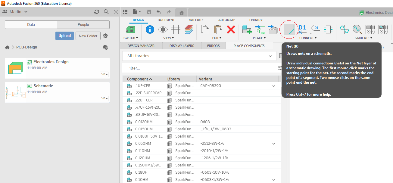
Use the Net tool to make connections (see below)
and using a combination of dragging the mouse and clicking to change direction or connect to an existing net. Use the following animated graphic as a guide. If you get a warning about "merging net segment into supply net" you should click Yes (see below).
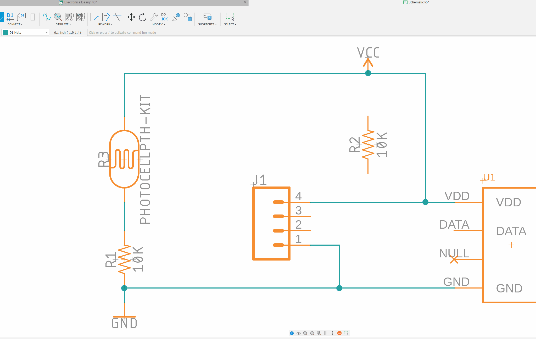
Finally, connect the data lines to the header pins as shown in the animation below. The circuit uses a 10 kiloOhm ‘Pullup' resistor on the data line of the DHT-22, which is recommended practice, although not always essential.
Save the schematic.
Your final schematic should look like the image below.
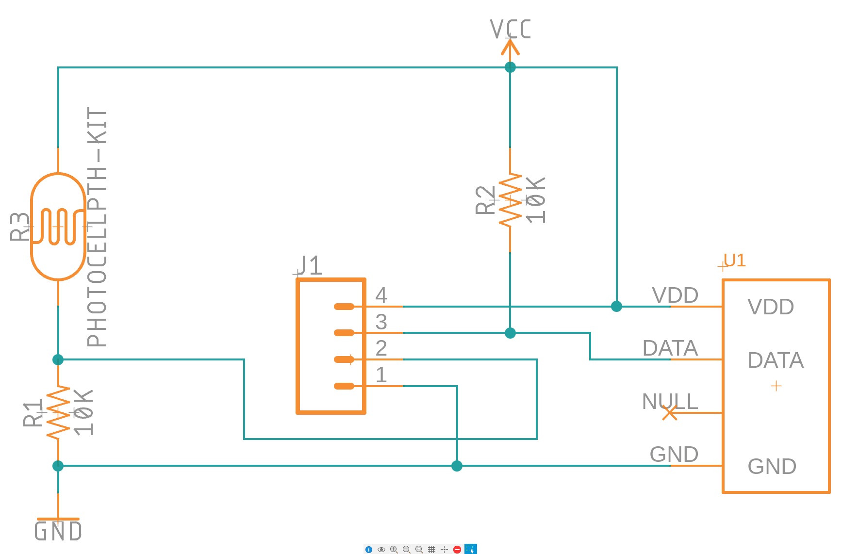
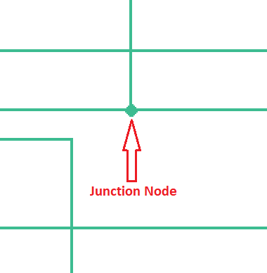
It is worth noting that crossed wires are only connected when a junction node is present (see below).
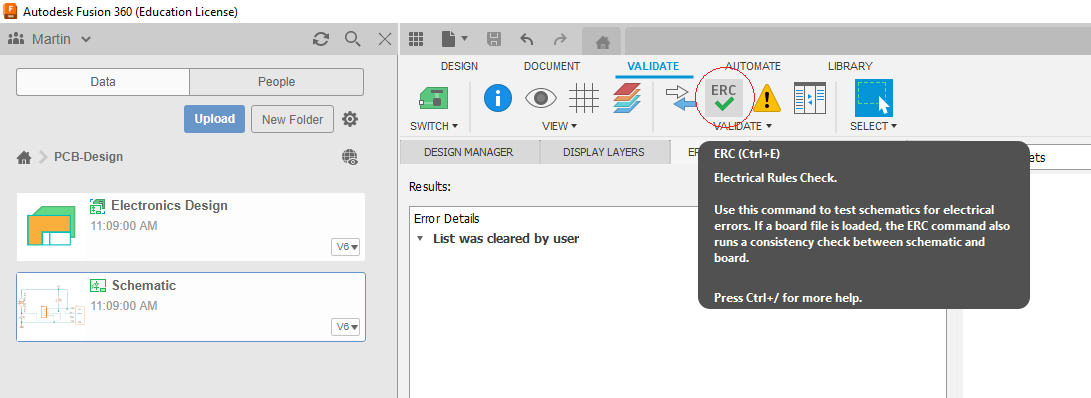
Once you have finalised your schematic, it is good practice to run an Electrical Rules Check (ERC) check. Click on the ERC button under the Validate tab (see below).
The results of the check should look something like this.
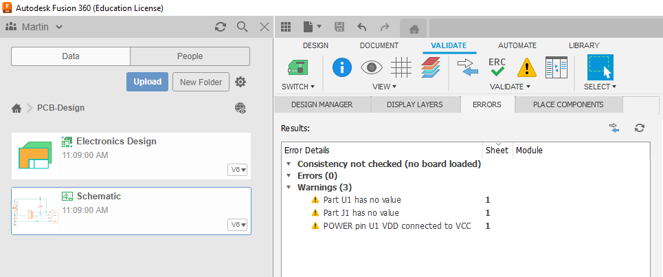
The warnings can be ignored, but if you see any errors you should investigate the cause. If you have no errors then save the schematic.
If you are still having problems with your schematic you may find the SparkFun Eagle schematic tutorial helpful.
In this part you will learn how to use Fusion 360/Eagle to convert your schematic from Part 1 into a PCB layout suitable for a PCB fabrication house to manufacture.
What You'll Learn
- Introduction to PCBs
- Creating a board from a schematic
- Setting the grid
- Setting the board dimensions
- Positioning the parts
- Routing traces
- Silk screens
- Running the Design Rule Check (DRC) tool
- Generating Gerber files
- Final words
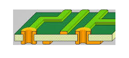
A printed circuit board (PCB) is composed of a number of layers (see below).
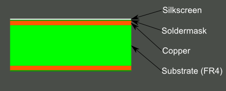
In the middle of the ‘sandwich' is the substrate, made of an insulating material such as fibreglass. For a two layer board, the top and bottom of the substrate is coated with a layer of copper to form the conducting traces, which are etched into the circuit pattern according to the board layout design. The copper layer is protected from damage and inadvertant short circuits by a thin insulating layer known as the solder mask. Finally, the silkscreen layer is applied on top of the solder masks to support the printing of text and graphics such as company logos and other information.
The Fusion 360/Eagle board editor includes numerous other virtual layers, representing drill holes and board dimensions etc, however most can be ignored for simple PCB layouts. Drill holes and a basic silkscreen are automatically generated by Fusion 360/Eagle from the parts included in the Schematic.
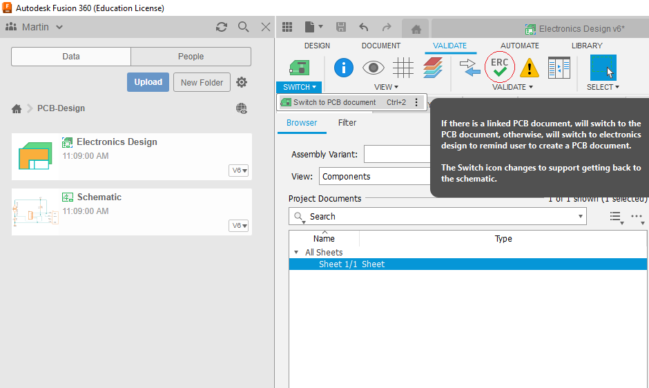
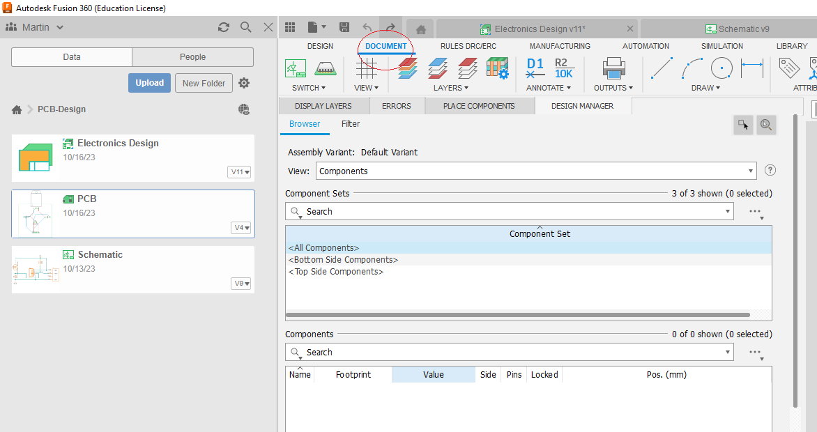
We are now going to use the schematic (circuit diagram) to inform our actual PCB design. Use the Switch button to generates a board and switch to the board editor view (see below).
You should now see the board editor view (see below).
From now on we will be working with the board editor view (although it is important to keep both the Schematic and Board view open, so that your project remains in sync).
First we switch the grid to mm (instead of inches) using the Grid button as shown below
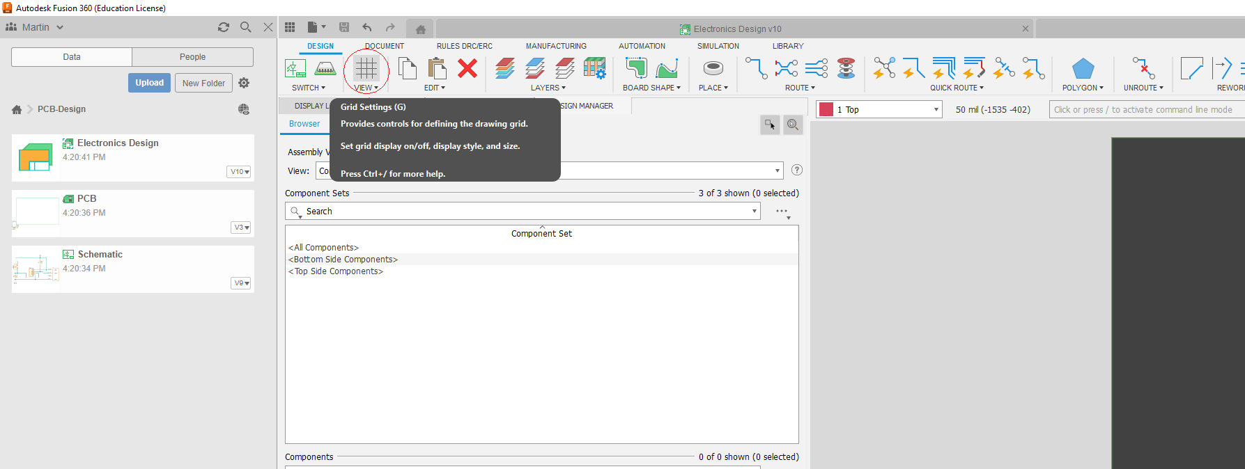
and use the resulting window to set the main grid to 1 mm resolution and the Alt grid to 0.1 mm (see below).
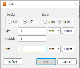
It is sometimes useful to use the finer resolution Alt grid when positioning parts or labels. You can switch to the Alt grid at any time by holding down the Alt key on your keyboard.
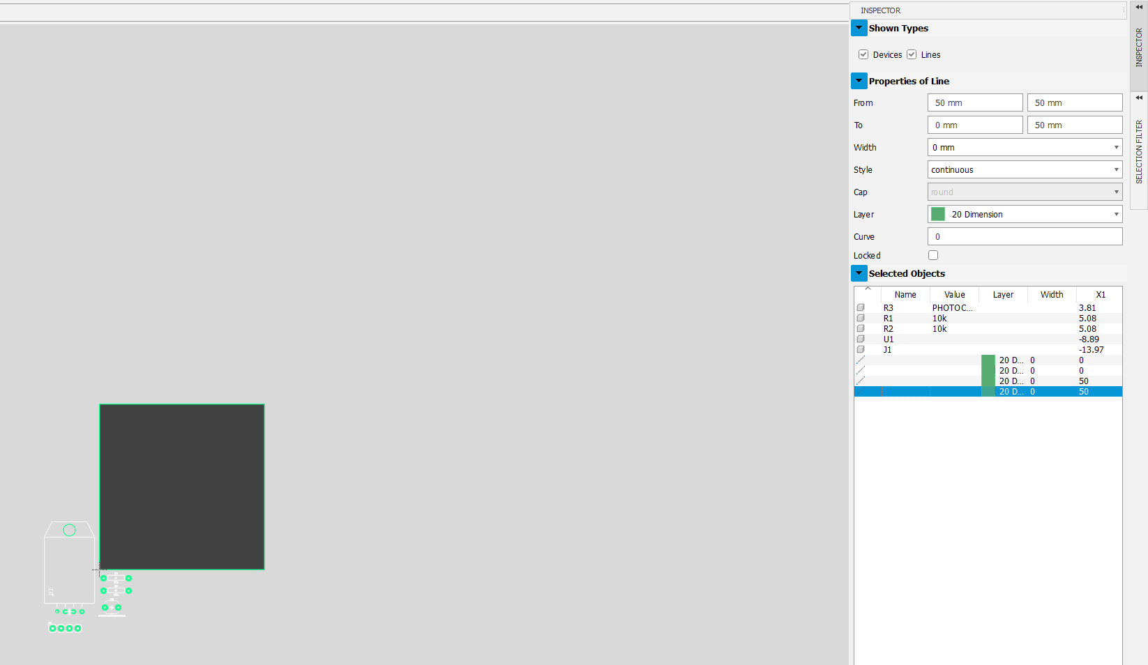
One of the first tasks to do is to set the dimensions of your board. This will often be determined by external factors such the dimensions of the enclosure you intend to use for your project. Here we will arbitrarily set the board dimensions to approximately 5 cm by 5 cm, that is 50 mm x 50 mm.
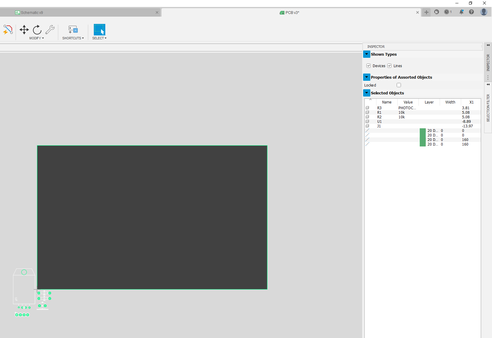
Firstly, choose the Select tool and select the board (see below).
then open the Inspector panel (see below)
Now select the edges of the board and edit the length (to, from) (see below)
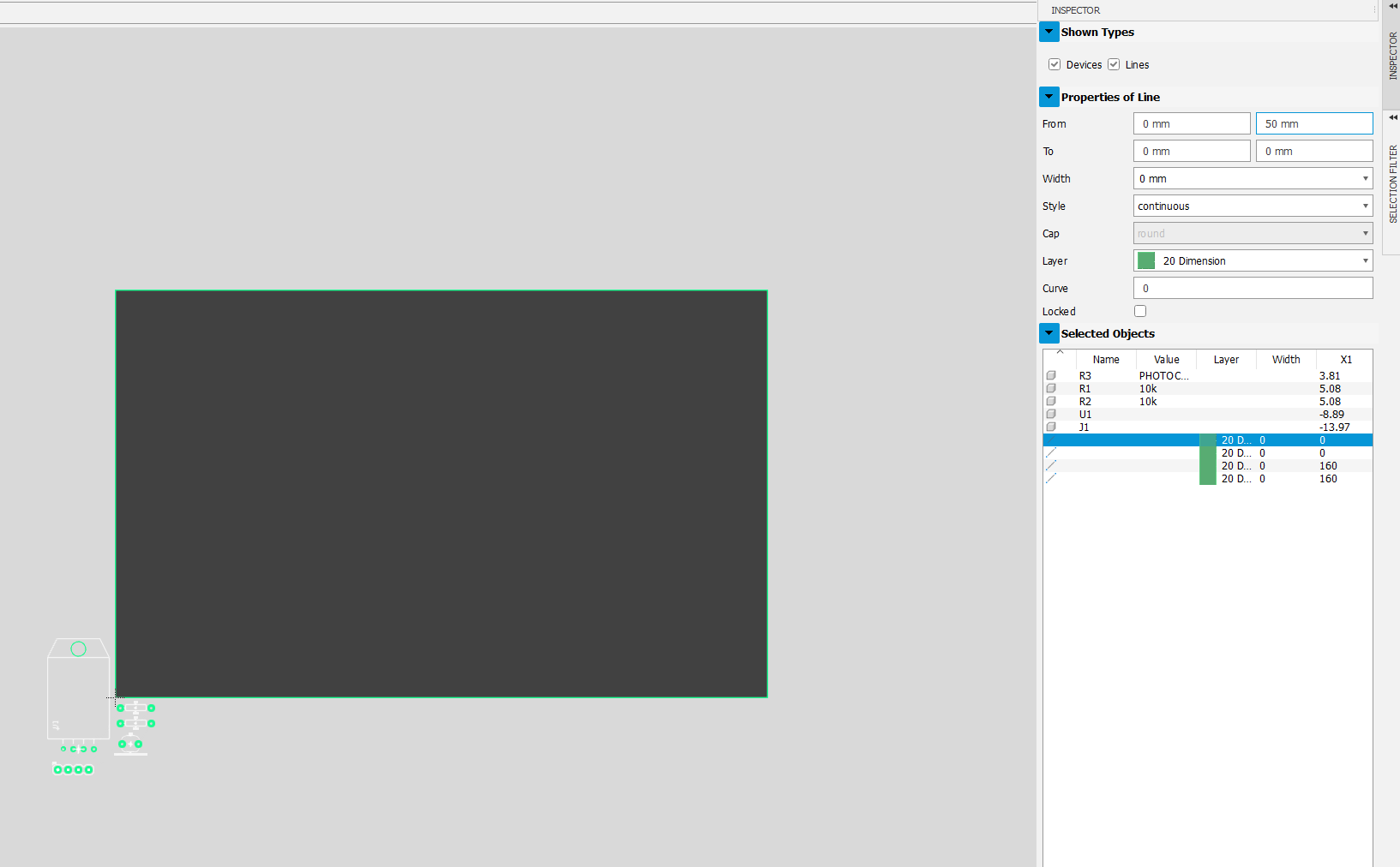
After editing all four edges the board should look like this
When finished Save your board layout.
Now we will arrange the parts on the board using the Move tool. To move a part click on its cross-hair and then drag it to the position you want (see below).
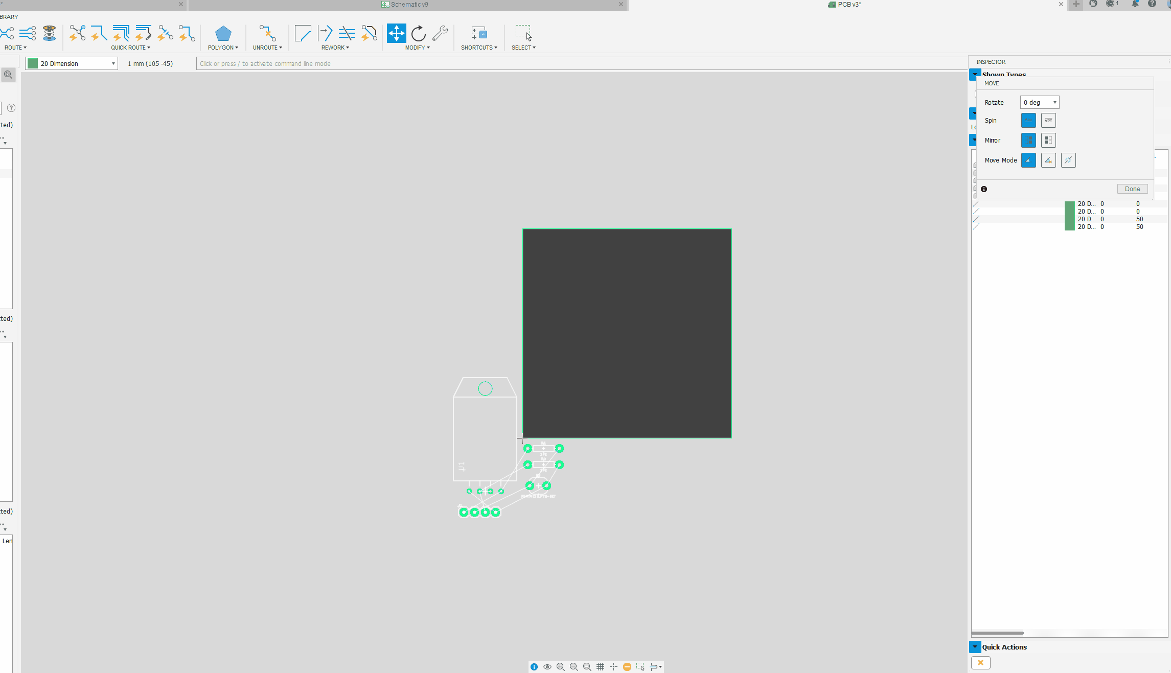
In a simple example like this the positon of the parts on the board is not critical - and you can always re-arrange them later with move and rotate. When finished Save your board layout.
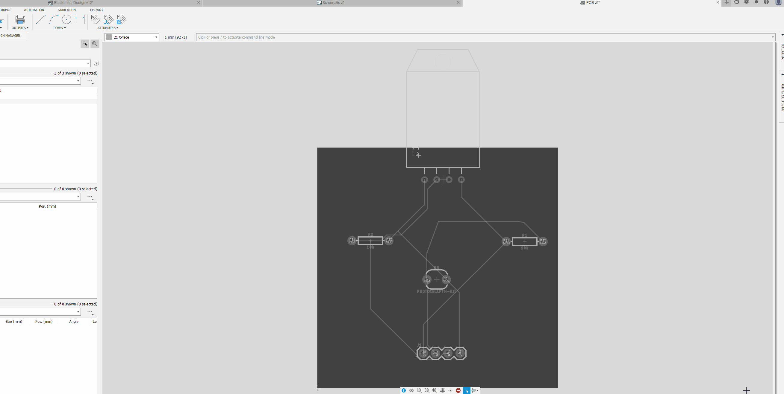
However, you will notice that some connections (‘air wires') cross each other. This is a problem for a PCB as the resulting copper traces would cross, causing short circuits. To avoid this PCBs employ two copper layers: one on the top; and one on the bottom. If necessary, traces on the top and bottom layer are electrically connected by a copper plated hole through the board known as a ‘Via' (see below)
Although in this simple example we don't need to use vias.
Routing is the process of converting ‘air wires' (the connections derived from the schematic) into copper traces on the PCB.
Fusion 360/Eagle contains a tool for automatic routing that works pretty well, particularly for simple circuits. Click on the Autorouter button as shown below.
The Autorouter displays the number of routing variations it will attempt (5 in this case). Click Start to initiate the Autorouter (see below).
For a simple circuit like this the Autorouter should finish within a couple of seconds. Click End Job to close the window (see below).
Your board editor view should look something like this (see below), although it may not be identical.
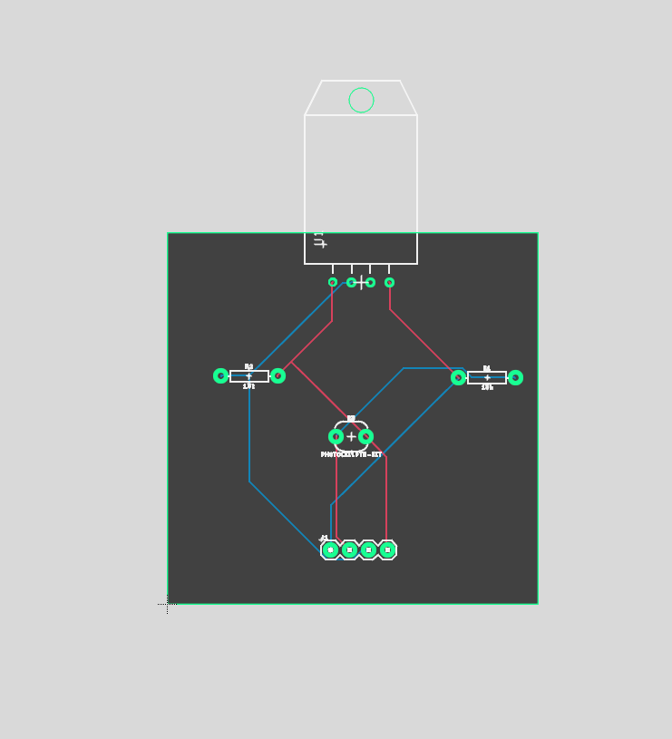
Tracks coloured red use the top copper layer of the board, while those coloured blue use the bottom layer.
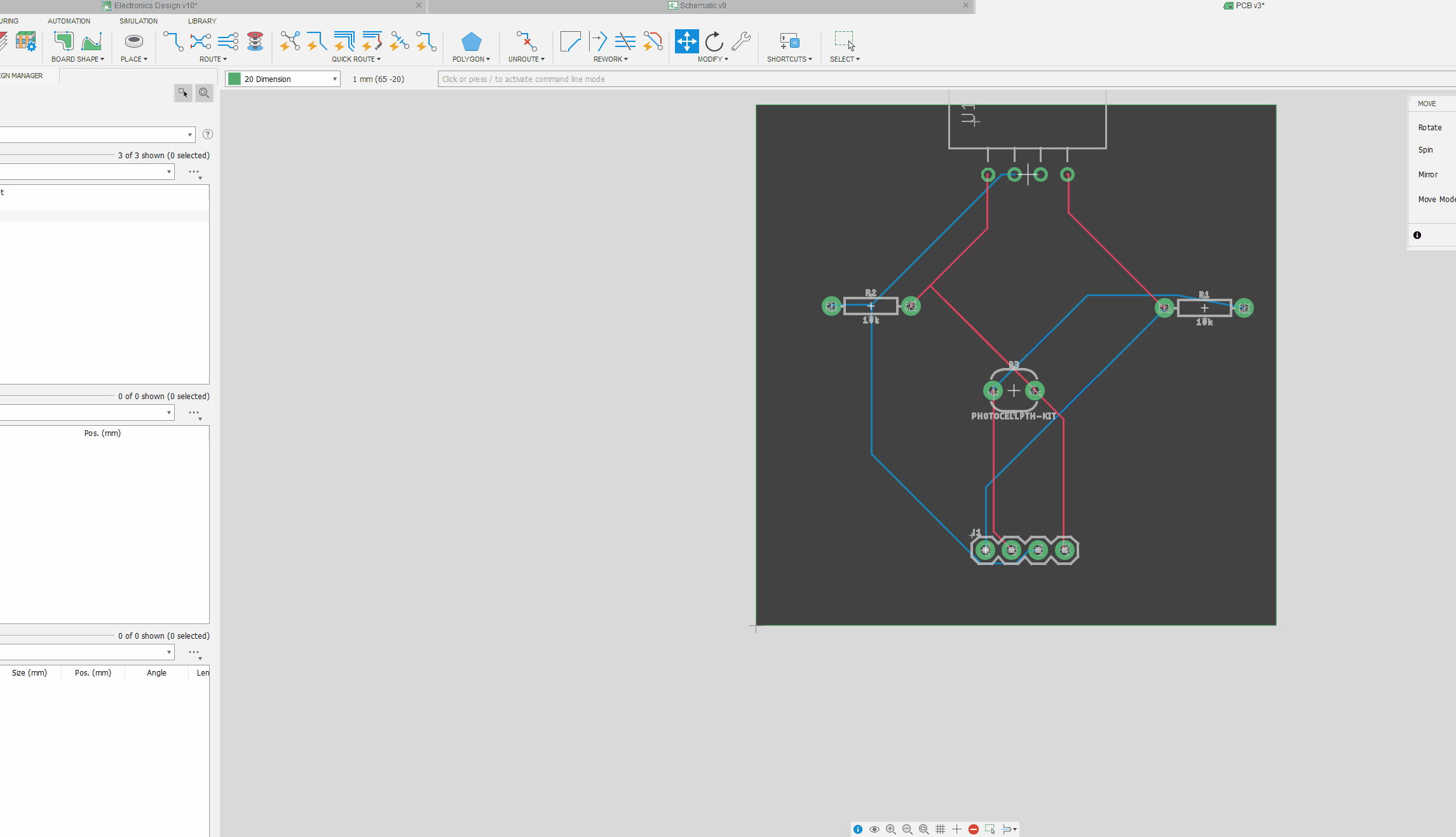
You can use the Move tool to drag trace around should you wish (see below).
When finished Save your board layout.
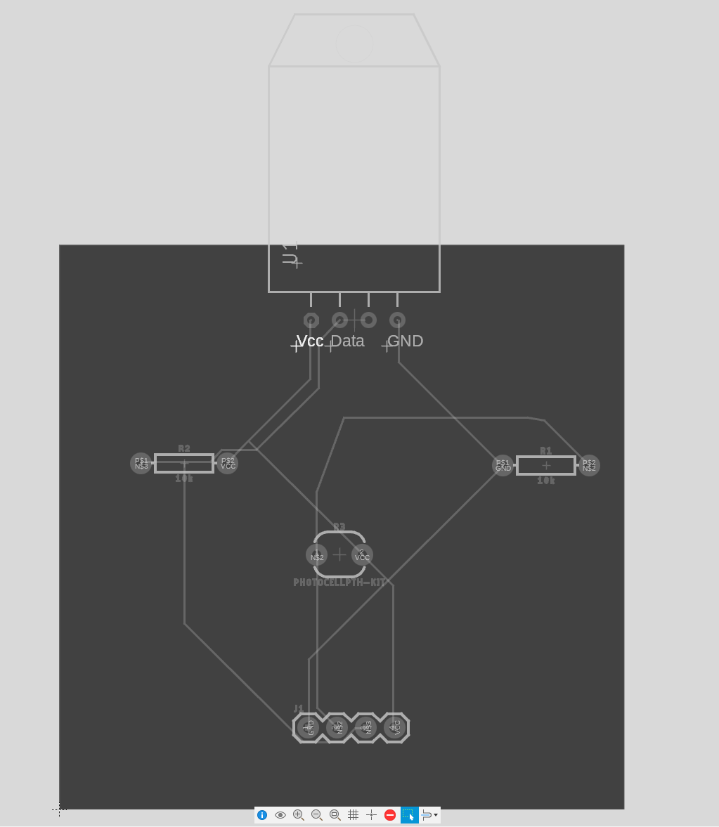
The silk screen layer allows additional text or patterns to be printed on the board. These are often company names and logos, but can also include additional circuit annotations. Here, we will add some labels to identify the header pins and DHT-22 connections.
The top silk screen layer is referred to as tPlace, the bottom silk screen layer is bPlace.
First select Single Layer Mode (see below).
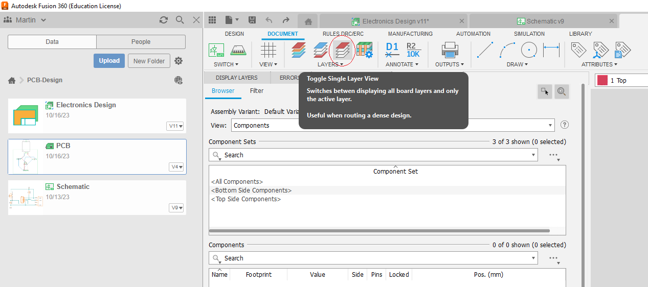
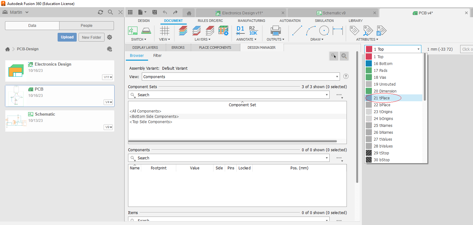
Then set the layer to tPlace as shown below
Now select the Document tab (see below)
And bring up the Text tool to create a label for ‘GND' to the DHT-22 (see below)
and add it to the board. You can resize the label by right clicking on it and changing its size in the Properties view.
Now add labels for the DHT-22 pins, from left to right, ‘Vcc' and ‘Data' (see below).
Now add labels to the header pins, from left to right, for ‘GND, ‘A2', ‘D2' and ‘Vcc' so that your board view looks something like this (see below)
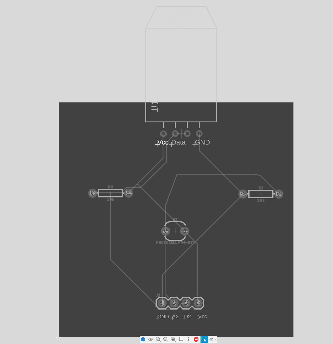
When finished Save your board layout.
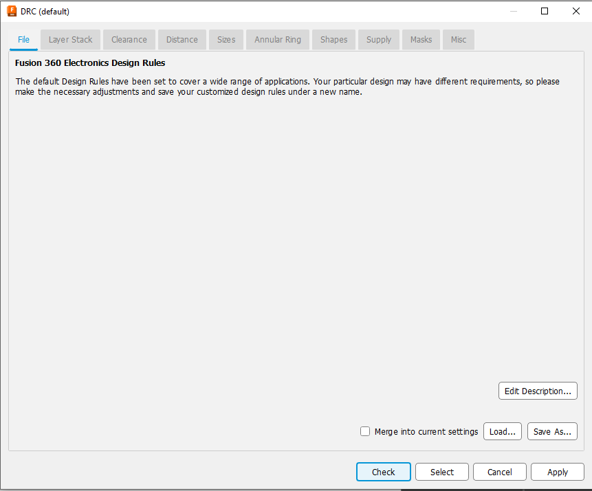
It is important to run a Design Rule Check (DRC) on your final board layout. This checks your layout against a set of Design Rules which specify things like the minimum width of traces, minimum spacing (clearance) between traces, minimum drill hole size etc. The DRC can detect errors in your layout such as overlapping or insufficiently seperated traces.
Some PCB fabrication houses supply their own design rules file which can be loaded into Fusion 360/Eagle. However, the default Eagle Design Rules are sufficient for most purposes and we will use it here.
To run a DRC select the Rules DRC/ERC and click on the DRC tool as shown below.
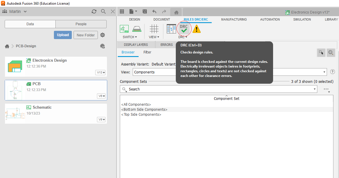
A new window will open up (see below) that displays the current rules (and allows you to modify them if you wish).
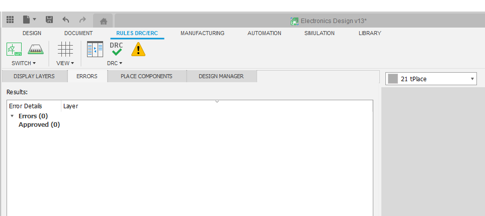
Click on the Check button to run the test. The results are displayed in the ERRORS tab of the left hand panel. For a simple circuit like this you shouldn't have any errors if you have followed the tutorial correctly.
The final step is to generate a set of Gerber files which can be sent to a PCB fabrication house. The Gerber format is an open standard used by PCB fabricators to describe the printed circuit board: it includes files to describe the copper layers, solder mask, drill hole data, silk screen etc.
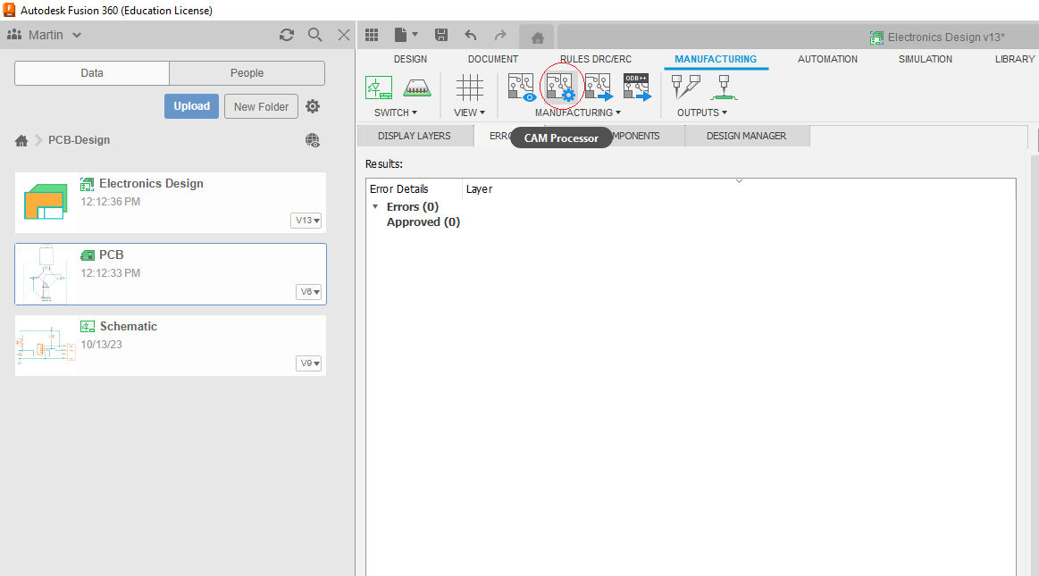
Fusion 360/Eagle uses a tool known as the CAM (Computer Aided Manufacture) Processor to generate the Gerber files from a board layout. Like the DRC, the CAM Processor relies on a set of rules (.cam file) to translate the board layout into a viable PCB. Often the PCB fabrication house will provide their own CAM file, which can be loaded into Eagle's CAM processor. However, Fusioin 360/Eagle comes pre-installed with suitable CAM files for some common PCB fabricators and in this example we will generate Gerber files suitable for Seeed Studio, a Chinese IoT component supplier and PCB fabricator.
Click on the CAM Processor launcher, found under the Manufacturing tab (as shown below)
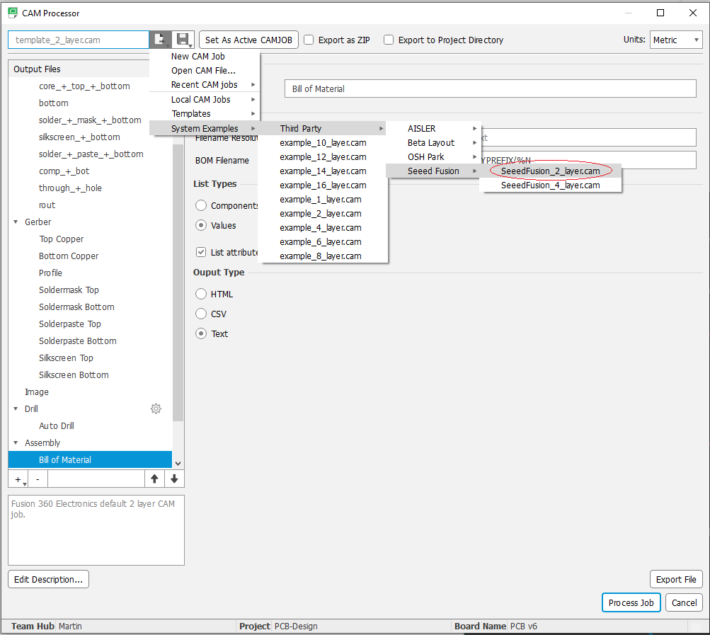
A new window will open. At the top left use the Load job file option to load the 2-layer CAM file for Seeed Fusion (the PCB manufacturing arm of Seeed Studio) as shown in the image below.
Once you have selected the CAM file, simply click on the Process Job button
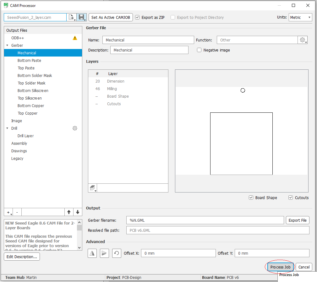
and save the generated zip file in an appropriate place.
This is as far as we will go in this tutorial. However, if in the future you wish to have a PCB fabricated, you would upload your zip file containing the Gerber files to the appropriate place on your fabricator's website and pay a fee. In the case of Seeed Studio it costs about £10.00 (including postage to the UK) for one design and a run of 10 identical boards (the minimum quantity) - delivery time being around 2 weeks. Other popular fabrications include JLCPCB and PCBWay. Some other fabricators such as OSH Park allow smaller runs as low as 3 copies.
This has been a very gentle introduction to designing PCBs, using a very simple circuit. Creating more complicated designs is a matter of practice and experience. SparkFun has a tutorial on board layout and PCB design which is worth looking at if you intend to create your own PCB.
Commercial PCBs often contain thousands of tiny, closely spaced surface mount parts and laying out such designs requires considerable skill and experience. However, as this is not a course in Electronic Engineering, whether you choose to create PCBs for your own projects or use an alternative approach such as stripboard is a matter of personal choice.